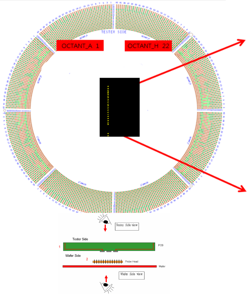
As part of IC development there is the “unpleasant” part of bringing the device to production with ATE. ATE testing is integral part of the product flow.
We work with many HW vendors (Form Factor, Techoprobe, MPI, SV-probe) to build and manufacture load board for CP (Chip Probe) and package parts
Our job is to convert “DESIGN INFORMATION” into “BOARD DESIGN INFORMATION” while adding the necessary on board circuitry around the DUT

We try to automate most of the flow to mitigate errors. For instance we use tools to automate the extract of pads coordinates from gds file or cadence DB. This is a critical aspect of ATE design specially for vertical high density probe card where the cost can easily exceed 160K$.
Contact Us for more information